Why we’re ditching the big ovens for IR curing
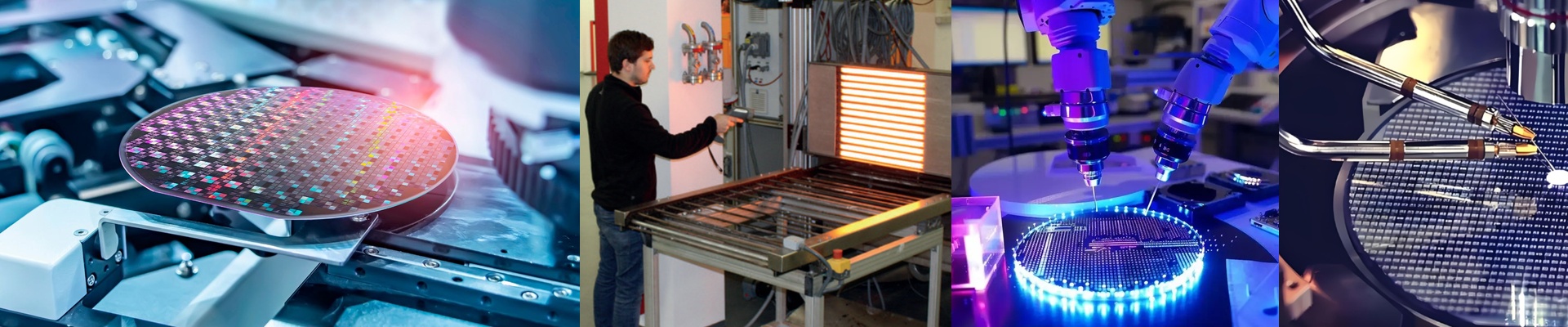
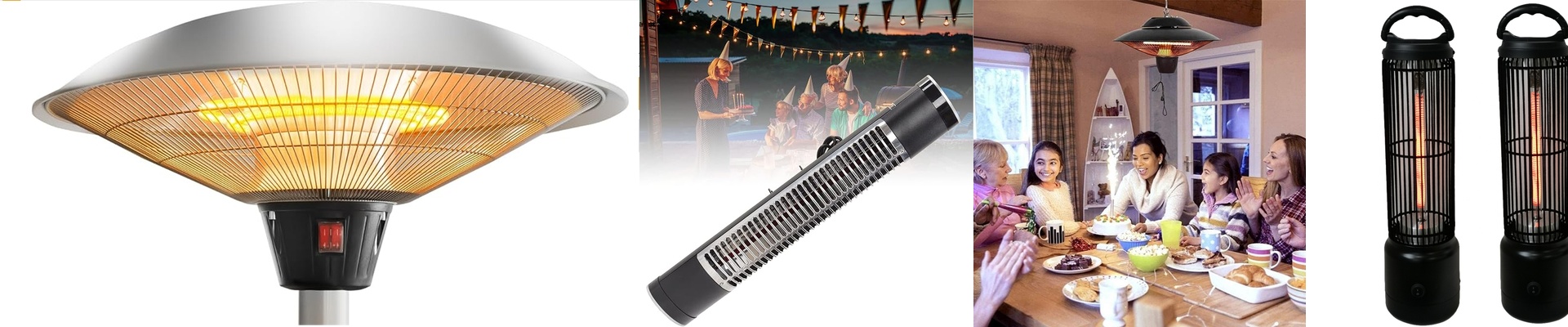
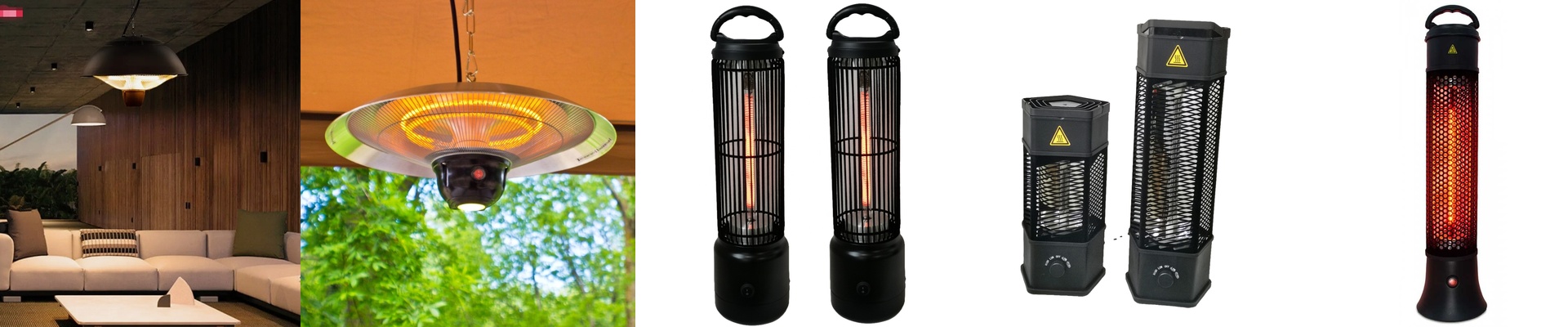
Let’s be honest: those old-school convection ovens are a bit of a dinosaur in the semiconductor world. They’re bulky, slow, and honestly, a pain to manage. That’s why so many fabs are switching over to infrared (IR) curing. It’s not just about following those “eco-friendly” rules or getting rid of lead—it’s about actually making the process work better. Here’s the thing about how this works. With a convection oven, you’re basically trying to heat up a massive room full of air just to get some energy onto a tiny wafer. It’s inefficient. IR is different. It’s direct. The energy jumps straight from the source to the substrate. No middleman. No waiting around for the air to warm up. Because it’s so direct, you can stop relying on those nasty organic solvents or lead-based flux accelerators just to speed things up. Plus, your power bill takes a hit—in a good way. We’re talking about cutting energy use by 30% to 50%. And if you’ve ever spent time in a cleanroom, you know the nightmare of particulates. High-velocity fans are basically dust-blowers. IR heaters just sit there. They’re static. No moving air, no flying contaminants, and no combustion fumes leaking into your controlled space. It’s just a clean, quiet, closed-loop process. But look, it’s not magic. There are a few things you have to get right. IR is fast. Really fast. You can hit your curing temps in seconds. But that speed is a double-edged sword. If your wafer isn’t centered or the intensity is cranked too high, you’ll get “hot spots.” One wrong move and you’ve warped your substrate. You’ve got to be picky about your PID controllers and distance sensors, or you’re just going to burn through your materials. The best part, though? The footprint. When you kill that long warm-up lag, your carbon footprint shrinks along with it. No greenhouse gases during the cycle, no massive electrical drain. It just fits into the fab and passes the green energy audits without any fuss. It’s just a simpler way to work.