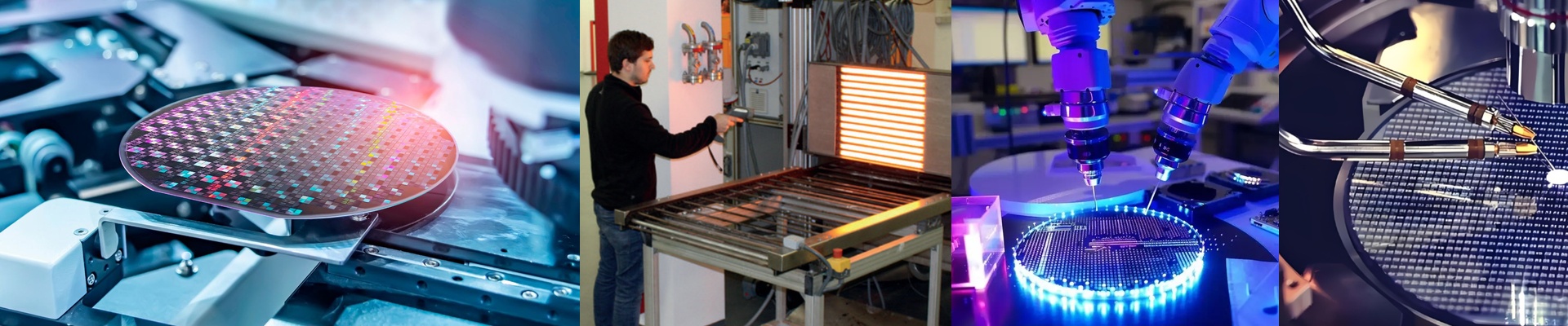
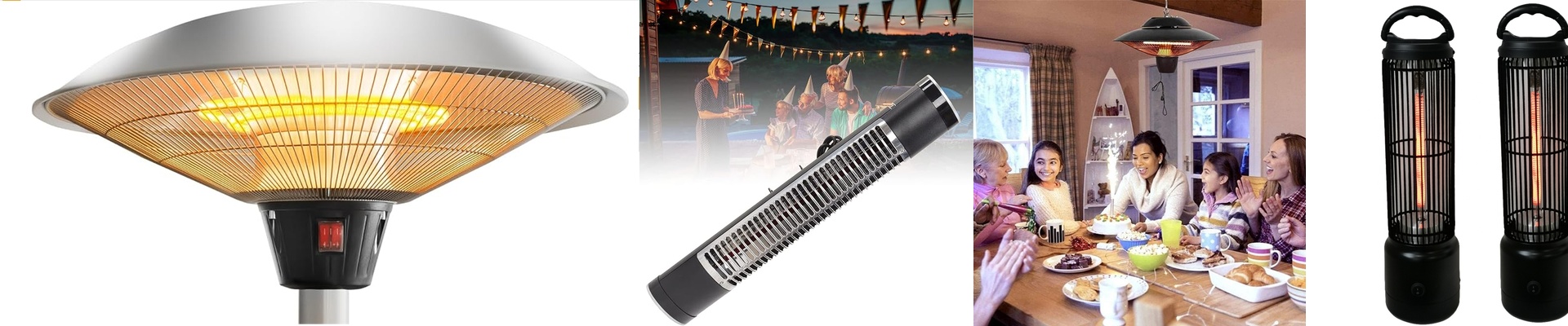
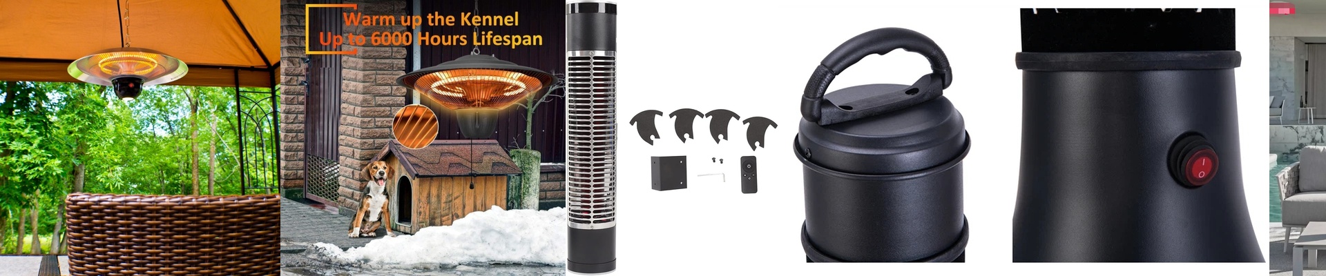
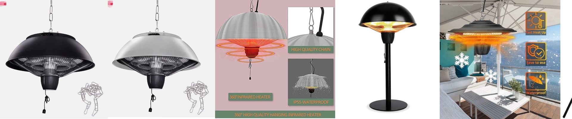
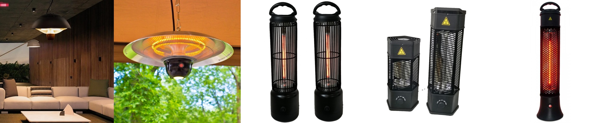
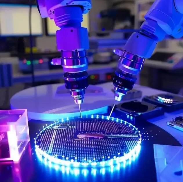
Out on the lithography floor, you know how it goes. A half-degree drift in the soft bake profile and your critical dimension is chasing nanometers. The line is suddenly walking away from you. We built the dimmable semiconductor heater lamp to keep the thermal budget where it needs to be—tight, repeatable, and under control. What matters under the hood The lamp leans on a short-wave infrared emitter, tuned for fast wafer heating, and holds wafer-level uniformity at ±0.1°C across the bake surface. Dimming is direct and linear, so you set the photoresist temperature without overshooting the chuck’s thermal mass. The design is cleanroom-ready for Class 1–100, with zero particle generation at the hot zone and a sealed quartz/ceramic interface that takes wet cleans and solvent exposure without flinching. In practice, soft bake and hard bake land on target within seconds, and the process window stays wide enough for advanced nodes. Here’s the thing with photoresist processing: repeatability is the only scoreboard that counts. The dimmable heater lamp locks the bake curve from lot to lot, cutting shot-to-shot CD variation and etch bias. Thermal settling is faster, which shaves cycle time without costing yield, and the low-profile build drops into existing coat/bake tracks with minimal rework. You also see lower energy use because the lamp only pulls the power needed for the setpoint, and the long emitter life stretches out the PM window. On packaging lines, that same control gives you consistent epoxy cure and fewer voids—because the temperature profile is no longer a guess. A couple of practical notes before you pull the trigger. Match the connector interface and verify the power supply ripple spec; the lamp is sensitive to voltage noise that can show up as temperature jitter. Give it a short burn-in to settle the emitter output, then double-check chuck reflector alignment to keep uniformity intact. Plan the thermal budget around the substrate stack—thick wafers and low-k films respond differently, so calibrate with a metrology wafer first.